
Low Logic is the second challenge in the Hardware Exploitation track on Hack The Box. This challenge is a brilliant reminder that hacking doesn’t always start with a terminal or a cyber tool — it can begin with something as deceptively simple as a picture of a circuit.
The challenge description includes - "I have this simple chip, I want you to understand how it's works and then give me the output."

Challenge: Low Level
Category: Hardware Exploitation
Difficulty: Very Easy
Points: 10
Link: Challenge Link
Initial Foothold
First things first, we grab the downloadable ZIP file provided with the challenge, aptly named Low Level.zip, and unzip it with the ever-reliable password (hackthebox):
unzip 'Low Level.zip'
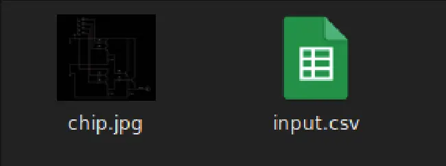
This drops us into a directory named hw_lowlogic, which contains two files:
cd hw_lowlogic
ls
Files received:
- chip.jpg — the star of the show
- input.csv — our digital test bench
We confirm their types using:
file *
File Breakdown
Chip.jpg
Opening this image reveals a simple but rich schematic diagram of a circuit.
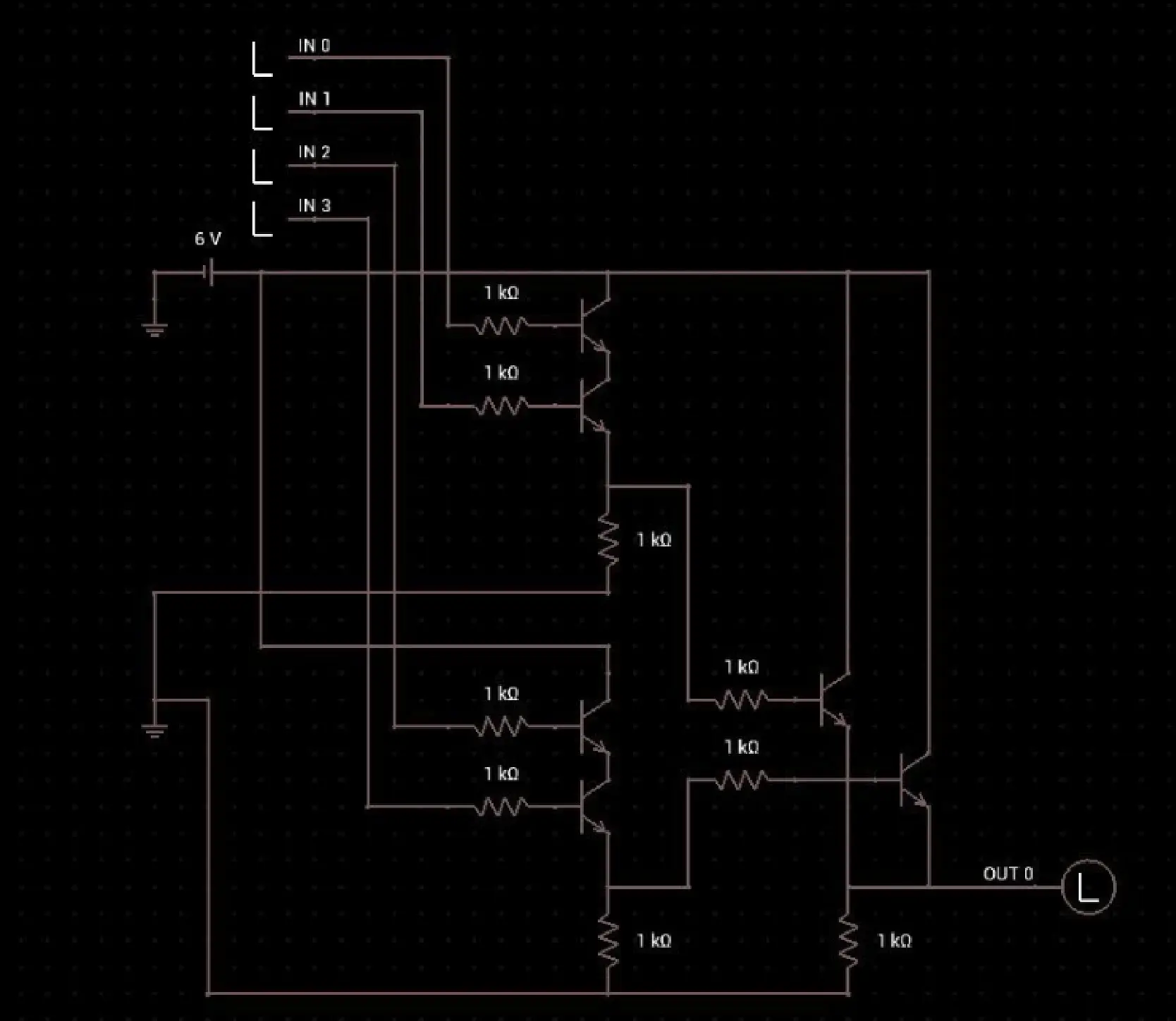
The diagram features four labeled inputs — IN0 to IN3 — flowing into what looks like a cluster of resistors and transistors, and finally resulting in a single output: OUT0.
The layout screams logic gates, and sure enough, once you squint a bit, you can identify the patterns of AND and OR gates built from transistors. It’s basically a visual puzzle that needs translating into logical operations.
Transistors are acting as logic switches here. When configured in series or parallel, they behave like ANDs and ORs respectively.
Let's go back to study the logic gates and its corresponding circuits.
AND Gate
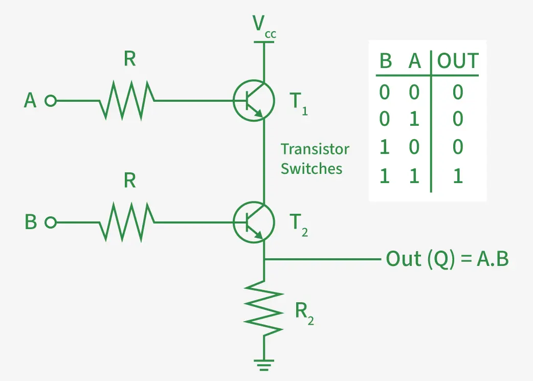
In the AND configuration:
- Two NPN transistors are connected in series.
- VCC goes to the collector of the first transistor (T1), which links to T2, then flows to ground.
- Inputs A and B go to their respective bases.
Only when both transistors are ON (inputs HIGH) does the current flow—just like a proper AND gate.
OR Gate
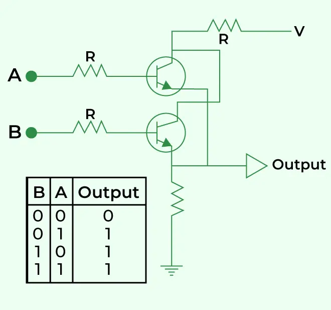
In the OR layout:
- Transistors are connected in parallel.
- If either transistor gets a HIGH input at its base, current flows to the output.
Classic OR gate behavior — if any one input is active, the output gets triggered.
NOT Gate
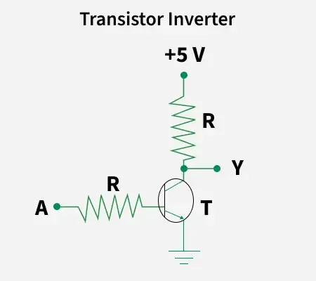
A single transistor can also invert a signal. When the input is LOW, the transistor is OFF, and output remains HIGH. When the input is HIGH, the transistor turns ON, grounding the output—producing a LOW. Now, you got yourself a NOT gate.
To learn more about logic gates, visit here.
input.csv
Now we check the contents of input.csv, which contains rows of binary input combinations:
head input.csv
in0,in1,in2,in3
1,0,0,1
1,1,0,0
0,1,1,0
0,0,1,0
1,1,0,1
1,0,0,1
0,0,0,0
0,0,1,0
0,0,0,0
Each row is a set of inputs for the circuit. Our task is to simulate the chip’s logic for each input row and generate the corresponding output.
Let's Decode the Logic
From our reverse-engineered schematic, we can deduce:
- IN0 and IN1 feed into an AND gate
- IN2 and IN3 feed into another AND gate
- The outputs of both are fed into an OR gate
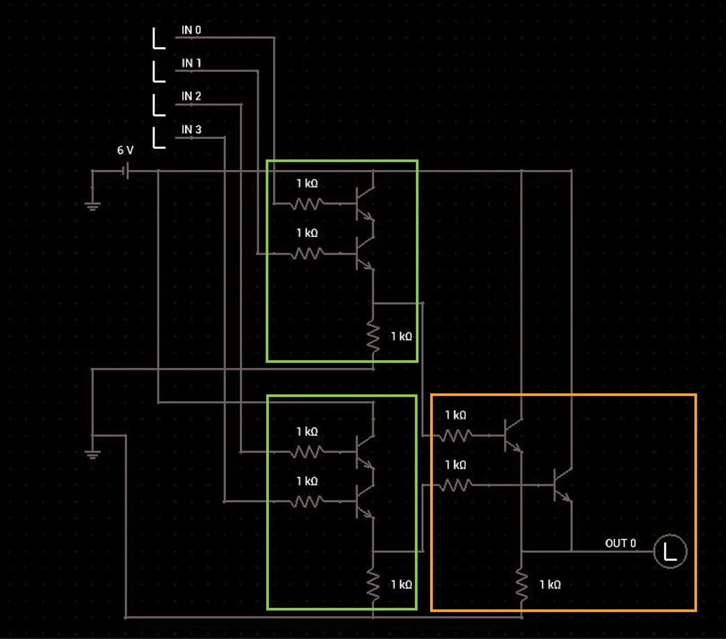
It’s like this in logic form:
OUT0 = (IN0 AND IN1) OR (IN2 AND IN3)
Here’s the Python script we used to do the heavy lifting:
import csv

def evaluate_logic_from_csv(file_path):
    output_bits = []

    # Open and read the CSV file
    with open(file_path, 'r') as file:
        reader = csv.reader(file)
        next(reader)  # Skip header row

        # Process each row of inputs
        for inputs in reader:
            in0 = int(inputs[0])
            in1 = int(inputs[1])
            in2 = int(inputs[2])
            in3 = int(inputs[3])

            # Apply logical AND to pairs
            result1 = in0 & in1
            result2 = in2 & in3

            # Combine results using logical OR
            final_result = result1 | result2

            # Store output as string
            output_bits.append(str(final_result))

    return ''.join(output_bits)

# Define input CSV and execute logic
input_csv = 'input.csv'
logic_output = evaluate_logic_from_csv(input_csv)

print(logic_output)
Output Extraction
Running the script gives us a nice binary blob:
010010000101010001000010011110110011010001011111010001110011000000110000011001000101111101000011011011010011000000110101010111110011001101111000001101000110110101110000011011000011001101111101
Now we decode it into ASCII:
python3 -c "s='010010000101010001000010011110110011010001011111010001110011000000110000011001000101111101000011011011010011000000110101010111110011001101111000001101000110110101110000011011000011001101111101';
print(''.join([chr(int(s[i:i+8], 2)) for i in range(0, len(s), 8)]))"
Found flag:
HTB{4_G00d_Cm05_3x4mpl3}

Conclusion
Low Logic is the kind of challenge that shows just how far a solid understanding of basic electronics and a bit of scripting can take you. There were no serial consoles to sniff or firmware to dump—just a JPG, a CSV, and a bit of brainpower. This was a perfect exercise in reading transistor-level logic, identifying gate behavior, and simulating the circuit’s truth table in code. It’s one of those challenges where hardware meets software in the best way possible.
Whether you’re new to hardware exploitation or just need a fun warm-up, Low Logic is proof that even the simplest-looking circuits can be hiding a flag—if you know where (and how) to look.